Alloy splitting of the defect electronic level
Au(-/O) and Pt(-/O) states in SiGe alloys. In red and blue colors are the spectra and alloy pattern diagrams measured for the gold and platinum acceptors in SiGe, respectively. The Laplace DLTS allowed to observe the alloy splitting coming from the first-nearest neighbours for the case of gold and from the first- and the second-nearest neighbours for the case of platinum [Phys. Rev. Lett. 83, 4582 (1999) (http://dx NULL.doi NULL.org/10 NULL.1103/PhysRevLett NULL.83 NULL.4582), Phys. Rev. B. 63, 235309 (2001) (http://dx NULL.doi NULL.org/10 NULL.1103/PhysRevB NULL.63 NULL.235309)].
[Top]
Laplace DLTS combined with uniaxial stress technique
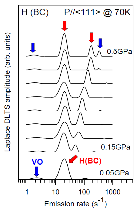
Uniaxial stress induced splitting of the Laplace DLTS peak related to the bond-centered hydrogen i n silicon (red arrows) and the vacancy-oxygen pair (blue arrows) observed in silicon after low-temperature proton implantation. The splitting pattern (3:1) indicates the trigonal symmetry of the hydrogen defect and the orthorhombic symmetry of the vacance-oxygen pair (splitting pattern 1:1).
Problems that can be solved with the Laplace DLTS combined with the uniaxial stress:
- defect symmetry,
- defect piezospectroscopic parameters (the lattice relaxation type),
- defect re-orientation, stability, short-range diffusion.
[Phys. Rev. Lett., 83, 4582 (1999) (http://dx NULL.doi NULL.org/10 NULL.1103/PhysRevLett NULL.83 NULL.4582)]
[Top]
Probing the epitaxial layer strain
![]() The Laplace DLTS spectra measured for the gold acceptor state in 2% strained and relaxed SiGe layers. The shift between these two spectra can be considered as being to due the planar strain in the epitaxial layer. From the known piezospectroscopic parameters of the defect this shift could be recalculated into strain of ε=1.8e-3 and planar stress of P=0.58 GPa (for Si).
The Laplace DLTS spectra measured for the gold acceptor state in 2% strained and relaxed SiGe layers. The shift between these two spectra can be considered as being to due the planar strain in the epitaxial layer. From the known piezospectroscopic parameters of the defect this shift could be recalculated into strain of ε=1.8e-3 and planar stress of P=0.58 GPa (for Si).
[J. Appl. Phys. 96, 4689 (2004) (http://dx NULL.doi NULL.org/10 NULL.1063/1 NULL.1794897)]
[Top]
Arrhenius-plot for defect identification/testing
The Laplace DLTS method allows to measure prcisly the emission rate of particular DLTS signal. Two different silicon samples measured at exactly the same thermodynamic conditions reveal two similar signals, which after precise Arrhenius-type measurements turned out not to be the same.
after electron irradiation at 70K
VO* → VO at 140K
after proton implantation at 70K
(C-H)I→ (C-H)II at 220K
[J. Appl. Phys. 96, 4689 (2004) (http://dx NULL.doi NULL.org/10 NULL.1063/1 NULL.1794897)]
[Phys. Rev. B 66, 235205 (2002) (http://dx NULL.doi NULL.org/10 NULL.1103/PhysRevB NULL.66 NULL.235205)]
[Top]
![]()
Energy-state distributions of the Pb centers at the (100), (110), and (111) Si/SiO2 interfaces
The energy distribution of the Pb centers at the (100), (110), and (111) the Si/SiO2 interface has been determined. For the (111) and (110) interface orientations the distributions are similar and centered at 0.38eV below the silicon conduction band. This is consistent with only Pb0 states being present. For the (100) orientation two types of the interface states are observed; one similar to the (111) and (110) orientations while the other has a negative-U character in which the emission rate versus surface potential dependence is qualitatively different from that observed for Pb0 and is presumed to be Pb1.
The figure shows the emission rates (a) and normalized DLTS signal amplitudes (b) observed for the Pb states at the Si/SiO2 interface with different orientations. The energy on the horizontal axis is the difference between the bottom of the conduction band and the Fermi level cross-point at the interface. The solid lines slope in (a) is 1/(kBT) (T=150K), while for the dashed line is 1/(2kBT).
[Appl. Phys. Lett. 92, 242104 (2008) (http://dx NULL.doi NULL.org/10 NULL.1063/1 NULL.2939001)]
[Top]