
start
scientific divisions
institute homepage
| Staff |
| Facilities |
| Nanostructure laboratory |
| Selected publications |
| Background | Presentations |
Facilities
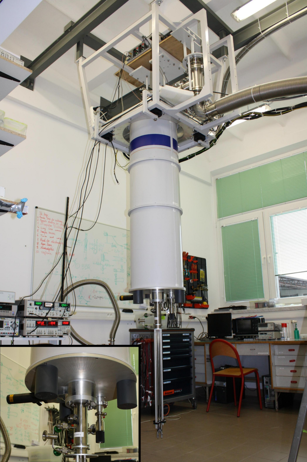
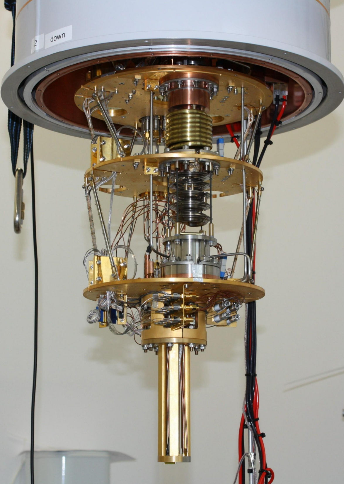
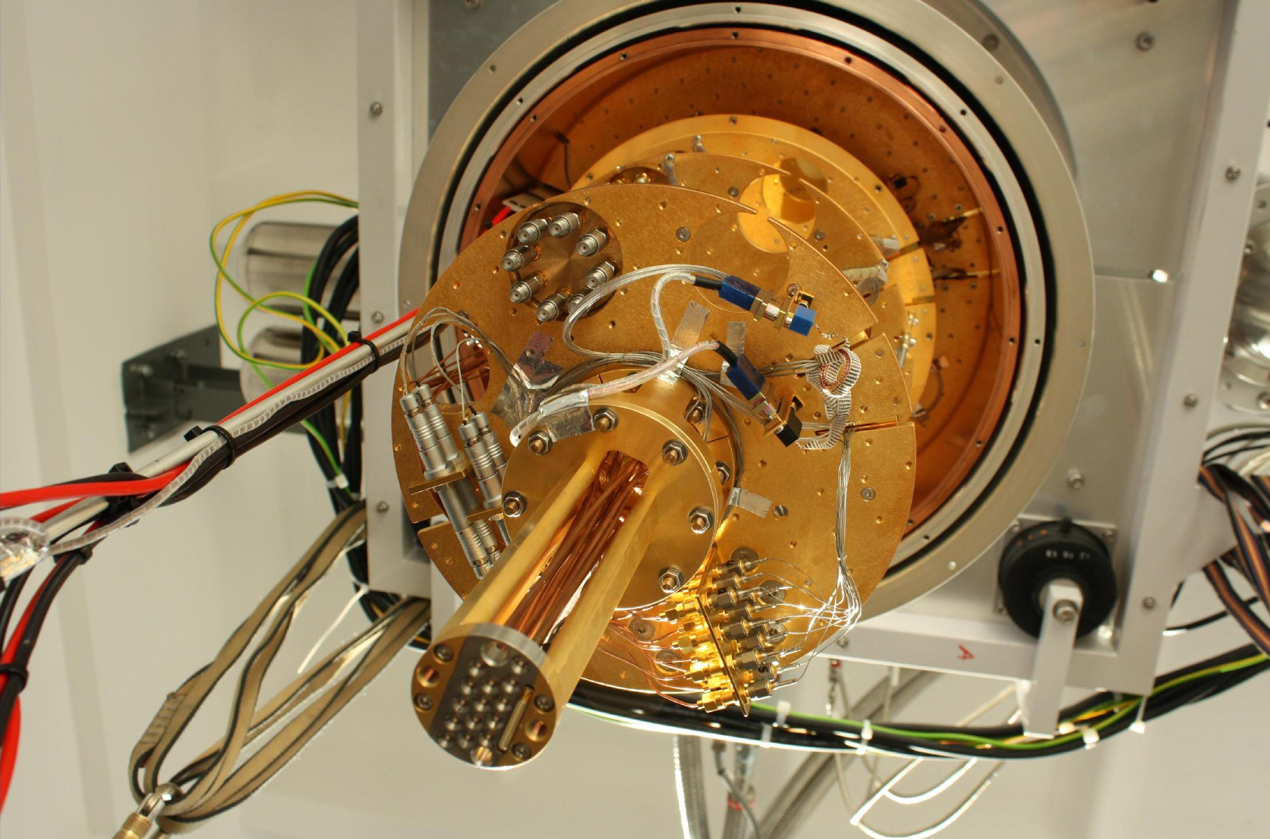
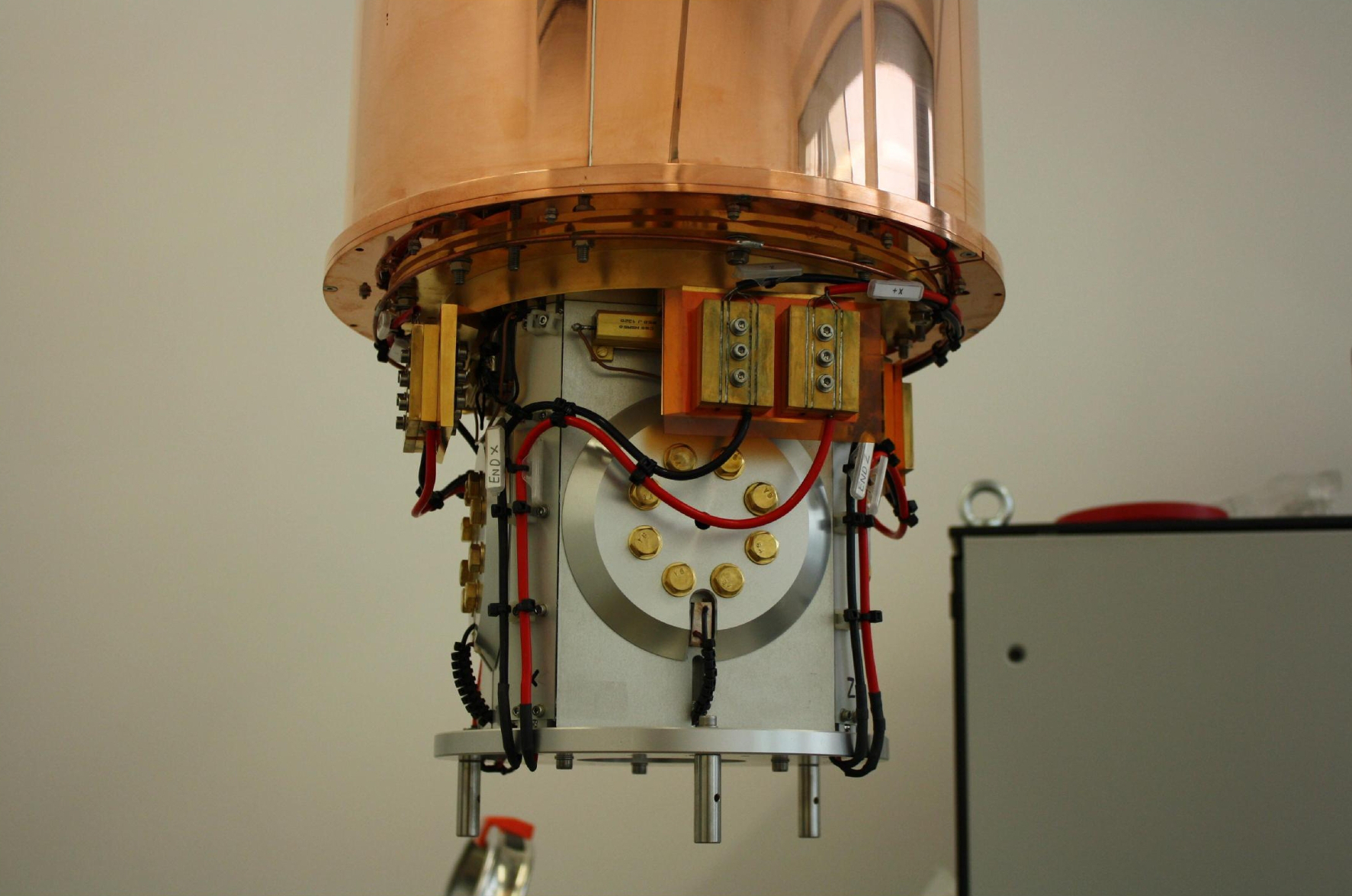
- Dry Dilution Refrigerator Triton 400/Oxford Instruments
Key parameters:
- Base temperature: < 10mK
- Cooling power at 100mK: 575µW
- Vector magnet: 6T-1T-1T
- Cryogen free, no liquid He4 required, cooled to ~ 4K with Pulse Tube Refrigerator
- Fully automated operation
- Bottom loader provides with fast sample exchange without need to warm up the whole system to the room temperature
- Cooling time from room temperature to 10mK:
- without magnet < 24h
- with magnet ~ 50h
- with fast loading ~ 10h
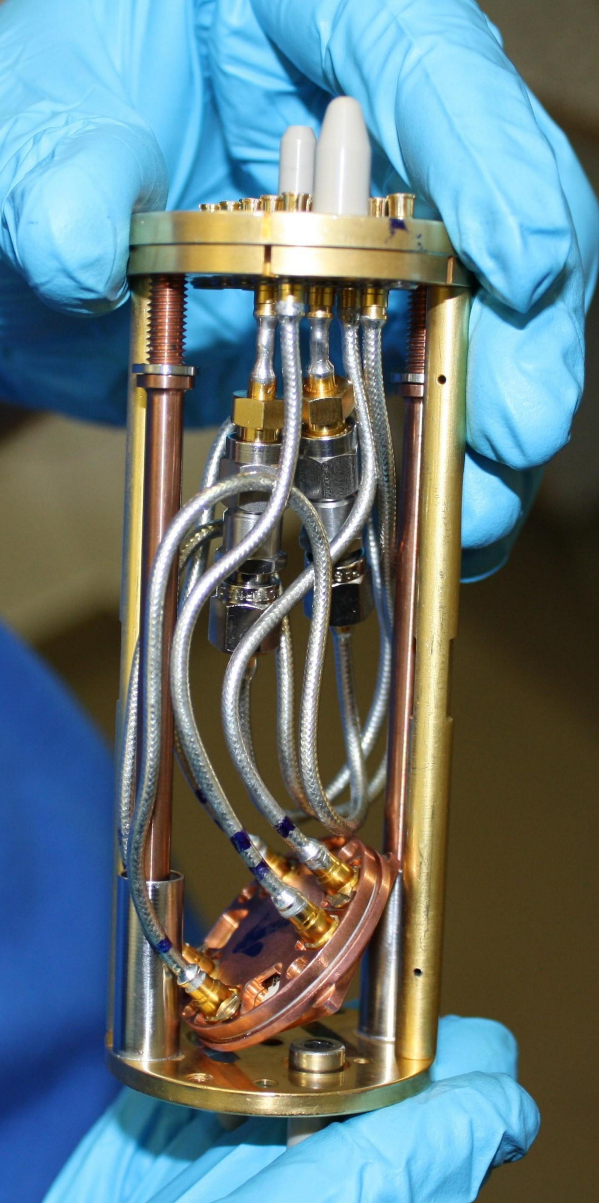
- The most wired fridge in the world:
- 8 microwave lines
- 12 Thermocoax lines
- 6 S1 coax lines
- 4 shielded twisted pairs
- Loom of 12 twisted pairs of Cu wires
- Loom of 12 twisted pairs of Cu/Supercon wires
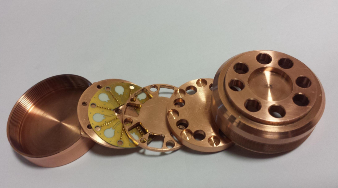
- Sample puck equipped with 14 SMP connectors and 51 pin DC Nanoconnector
- Temperature range:
- without magnet 10mK – 300K
- with magnet 10mK- 30K
- Cryogenic system (made by Cryoengineering Group SL-2.1 IF PAN Warsaw) equipped with 9 T superconducting magnet. It is designed for two different inserts: A) plastic dilution refrigerator He3/He4 (PDU-40 Nanoway, University of Jyvaskyla, Finland) with base temperature 30 mK and useful sample space diameter 20 mm. B) standard variable temperature insert for the range from 1.5 K to 300 K. Both inserts are used for transport measurements.
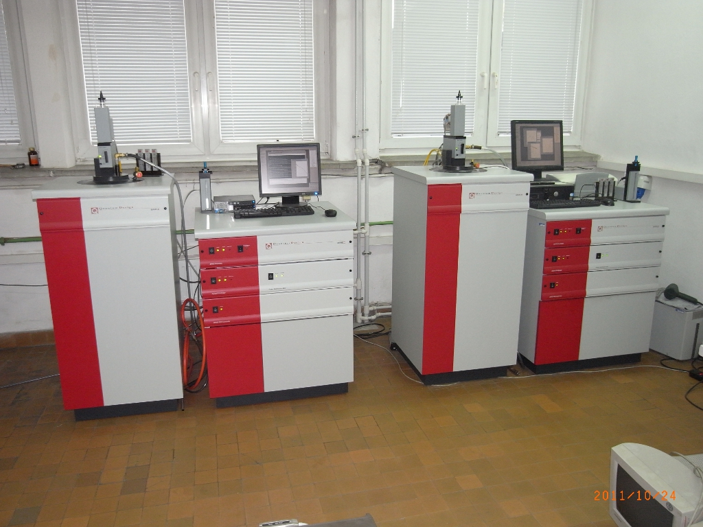
- Two SQUID magnetometers Quantum Design MPMS XL, 1.9 - 400 K (800K with added apparatus), up to 5T in AC, DC, RSO modes.
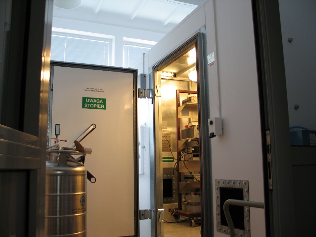
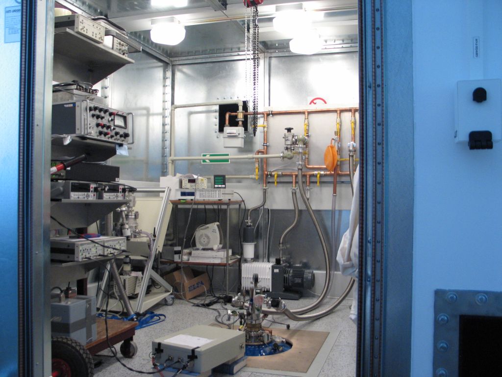
- He3 cryogenic system, made by Cryo Industries of America designed for electrical measurements in the temperature range from 0.25 to 300 K and in magnetic fields up to 6 T. Measured sample is placed in vacuum, on the cold finger. He3 hold time at base temperature is about 24 h. He3 insert external diameter 3’’, useful sample space up to 4?4?4 cm. The whole system is placed in e-m shielded room A1 class (shielding effectiveness 100 dB in the range 100 kHz – 5 GHz) made by Military Institute of Communication, Zegrze, Poland.
- Scanning electron microscope ZEISS Auriga - CrossBeam Workstation ( Ion imaging resolution of 2.5 nm at 30 kV, electron imaging resolution 1 nm at 15 kV ).
A reactive Gas Injection System for reactive ion etching (XeF2) and Pt/SiO2/W deposition. Nano-manipulators dedicated to electrical measurements and TEM sample preparation (Kleindiek, 0.5 nm resolution).
Electron/Ion beam lithography, (Raith Elphy Plus, Nanopatterning Engine).
Piezoelectric stage - high precision substage (Kleindiek, 0.5 nm resolution).
EDX - XFlash Silicon Drift Detector 5030 (Bruker) for low beam current applications,energy resolution of 127 eV. - Scanning electron microscope ZEISS EVO HD15 SEM: Emitter - LaB6, resolution - 2.0 nm at 30 kV.
HORIBA Jobin Yvon CL.
Kammrath & Weiss cryostat.
Peltier cryostat. - Scanning electron microscope JEOL 6400 ( 40 keV, 3.5 nm spot size ).
- Raith Elphy + e-beam lithography system in a clean room ( 16 bit DAC, vector scan writing mode, mark recognition and alignment, laser interferometer controlled stage with resolution 5 nm and overlay accuracy < 100 nm).
- Proximity corrections software.
- X - ray microprobe L200D Link ISIS.
- related processing infrastructure (hot plate/spinner, bonder, vacuum evaporator..)
SQUID magnetometers