Si(111) 7x7 surface. Various topography imaging of empty (left) and occupied (right) states (STM, 20 nm x 20 nm).
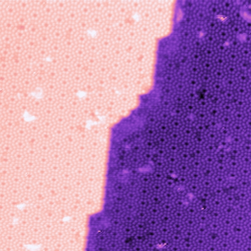

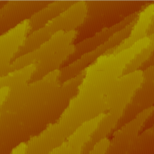
A monolayer step (left: 45 nm x 45 nm) and bunched steps (right: 500 nm x 500 nm) of Si(111) surface (STM).
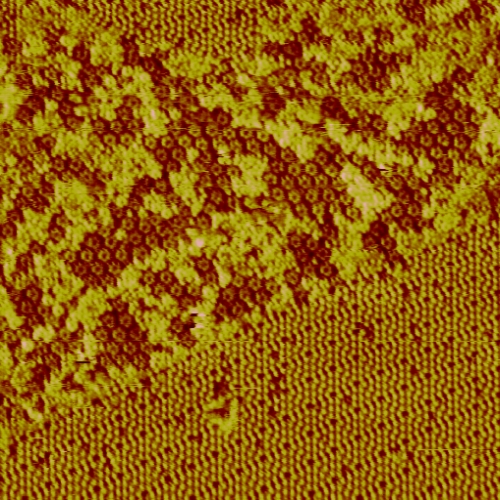
5x5 reconstruction of Si(111) surface visible in the central part of the image (STM, 50 nm x 50 nm).
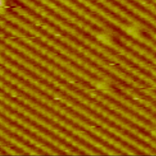
2x1 reconstruction of Si(100) surface (STM, left: 107 nm x 107 nm, right: 30 nm x 30 nm).

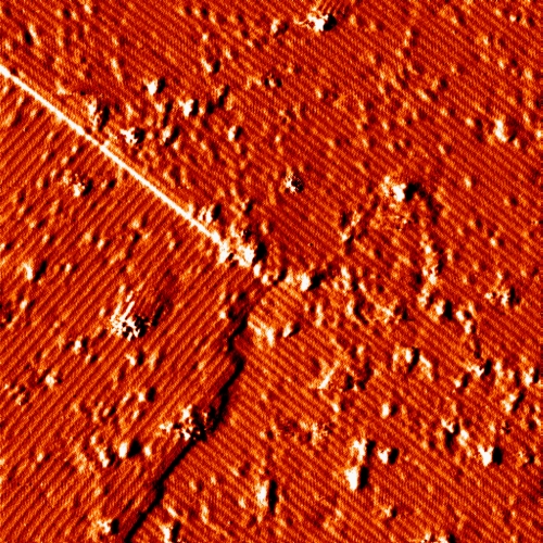
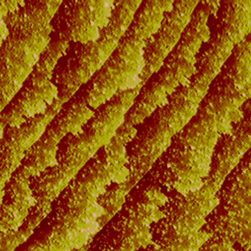
Left: Screw dislocations (pointed by arrows) on Si(100) vicinal surface (5 μm x 5 μm). Right: A single dislocation with a visible surface reconstruction (50 nm x 50 nm) (STM).
GaAs (100) surface cleaved in UHV (left: 50 nm x 50 nm, right: 7.2 nm x 7.2 nm) (STM).
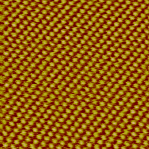
Topography image of graphite, HOPG (STM, 5 nm x 5 nm).
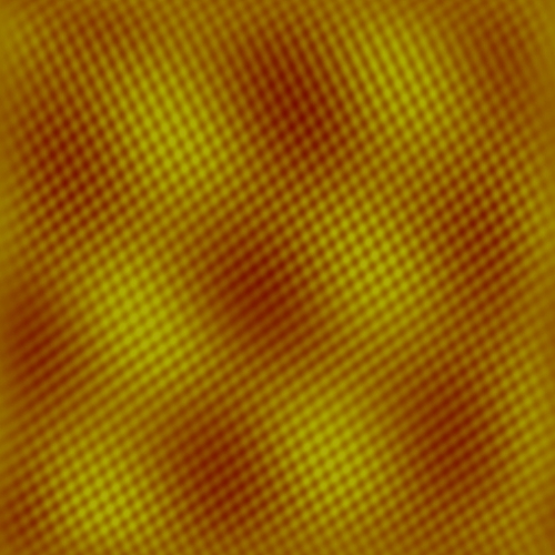
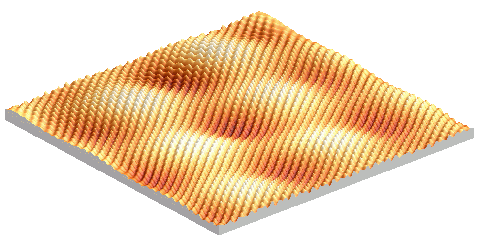
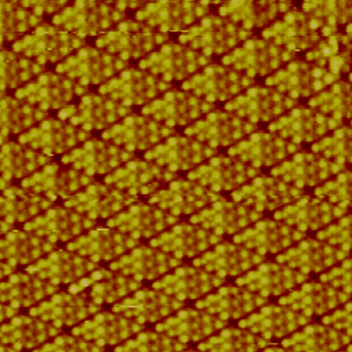
Superstructure on HOPG surface (left: 8.4 nm x 8.4 nm). Perspective view (right) (STM).
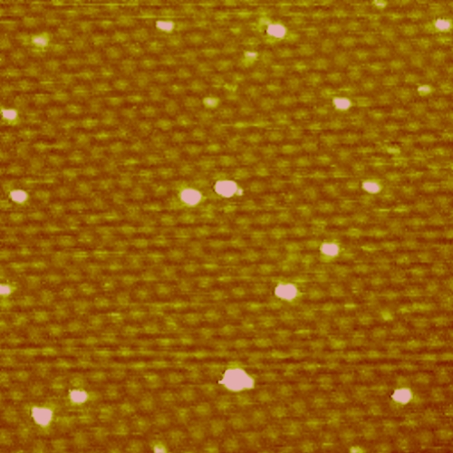
Ni nanoclusters on HOPG surface (80 nm x 80 nm). Does the HOPG superstructure influence distribution of the clusters?
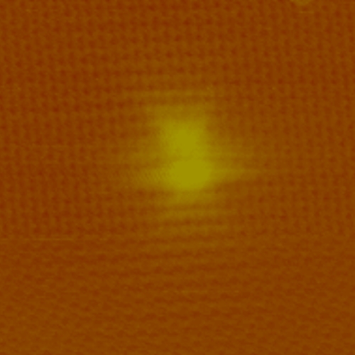
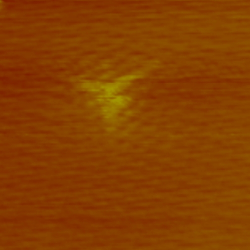
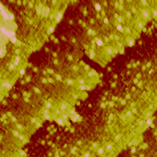
Disturbance of HOPG electronic structure by Ni (left: 7.5 nm x 7.5 nm) and Co (right: 7.2 nm x 7.2 nm) nanoclusters (STM).